- 您现在的位置:买卖IC网 > Sheet目录2007 > LTC491IS#TRPBF (Linear Technology)IC TXRX RS485 LOW POWER 14-SOIC
3
LTC491
491fa
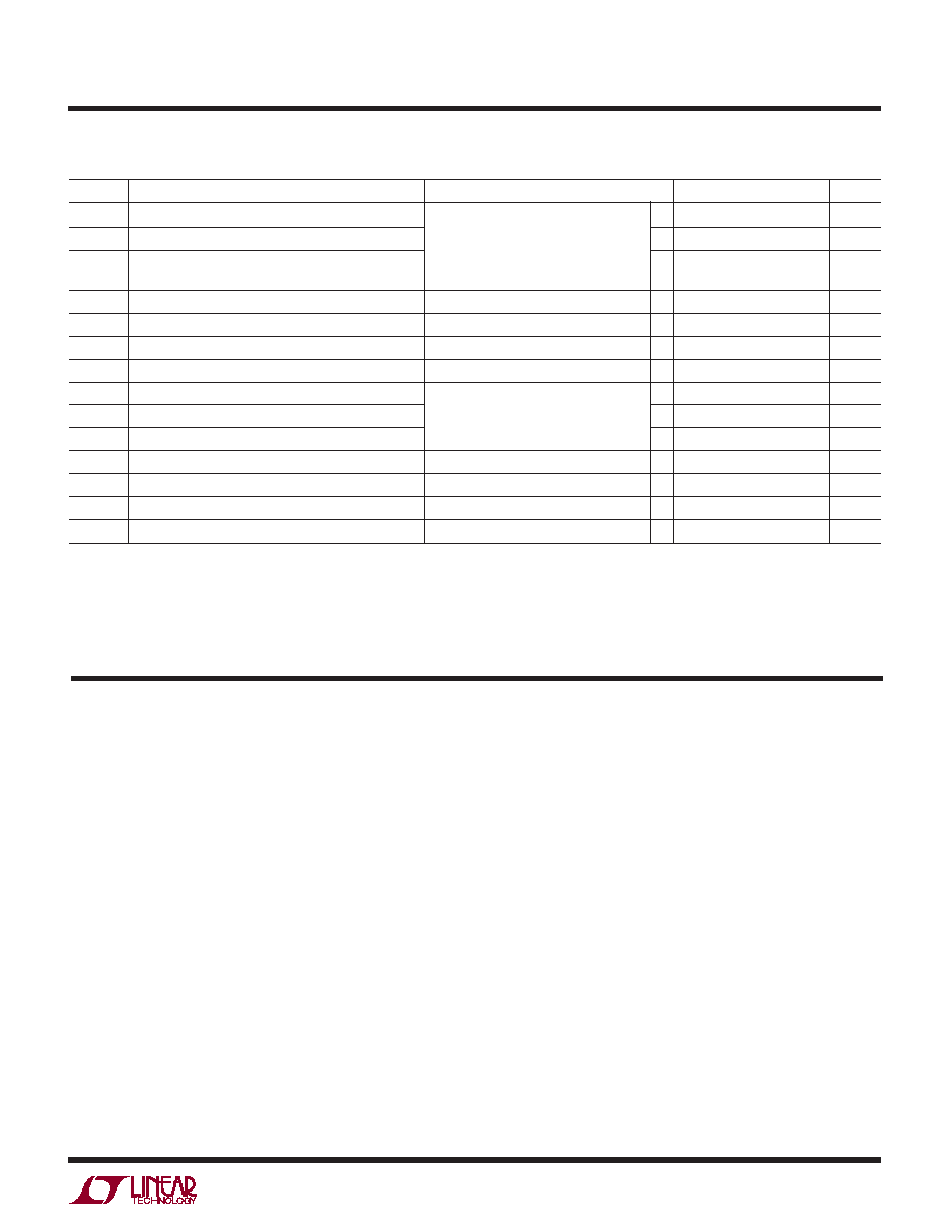
SYMBOL
PARAMETER
CONDITIONS
MIN
TYP
MAX
UNITS
tPLH
Driver Input to Output
RDIFF = 54, CL1 = CL2 = 100pF
q
10
30
50
ns
tPHL
Driver Input to Output
q
10
30
50
ns
tSKEW
Driver Output to Output
q
5ns
tr, tf
Driver Rise or Fall Time
q
515
25
ns
tZH
Driver Enable to Output High
CL = 100pF (Figures 4, 6) S2 Closed
q
40
70
ns
tZL
Driver Enable to Output Low
CL = 100pF (Figures 4, 6) S1 Closed
q
40
70
ns
tLZ
Driver Disable Time From Low
CL = 15pF (Figures 4, 6) S1 Closed
q
40
70
ns
tHZ
Driver Disable Time From High
CL = 15pF (Figures 4, 6) S2 Closed
q
40
70
ns
tPLH
Receiver Input to Output
RDIFF = 54, CL1 = CL2 = 100pF
q
40
70
150
ns
tPHL
Receiver Input to Output
q
40
70
150
ns
tSKD
tPLH – tPHL Differential Receiver Skew
q
13
ns
tZL
Receiver Enable to Output Low
CL = 15pF (Figures 3, 8) S1 Closed
q
20
50
ns
tZH
Receiver Enable to Output High
CL = 15pF (Figures 3, 8) S2 Closed
q
20
50
ns
tLZ
Receiver Disable From Low
CL = 15pF (Figures 3, 8) S1 Closed
q
20
50
ns
tHZ
Receiver Disable From High
CL = 15pF (Figures 3, 8) S2 Closed
q
20
50
ns
S
U
GC
C
HARA TERISTICS
WITCHI
(Figures 2, 5)
(Figures 2, 7)
Note 3: All typicals are given for VCC = 5V and temperature = 25°C.
Note 1: Absolute Maximum Ratings are those values beyond which the life
of the device may be impaired.
Note 2: All currents into device pins are positive; all currents out of device
pins are negative. All voltages are referenced to device ground unless
otherwise specified.
NC (Pin 1): Not Connected.
R (Pin 2): Receiver Output. If the receiver output is enabled
(REB low), then if A > B by 200mV, R will be high. If A < B
by 200mV, then R will be low.
REB (Pin 3): Receiver Output Enable. A low enables the
receiver output, R. A high input forces the receiver output
into a high impedance state.
DE (Pin 4): Driver Output Enable. A high on DE enables the
driver outputs, Y and Z. A low input forces the driver
outputs into a high impedance state.
D (Pin 5): Driver Input. If the driver outputs are enabled
(DE high), then a low on D forces the driver outputs Y low
and Z high. A high on D will force Y high and Z low.
GND (Pin 6): Ground Connection.
GND (Pin 7): Ground Connection.
NC (Pin 8): Not Connected.
Y (Pin 9): Driver Output.
Z (Pin 10): Driver Output.
B (Pin 11): Receiver Input.
A (Pin 12): Receiver Input.
NC (Pin 13): Not Connected.
VCC (Pin 14): Positive Supply; 4.75V ≤ VCC ≤ 5.25V.
The q denotes the specifications which apply over the full operating
temperature range, otherwise specifications are at TA = 25°C. VCC = 5V ±5%
UU
U
PI FU CTIO S
发布紧急采购,3分钟左右您将得到回复。
相关PDF资料
LTC6900IS5#TR
IC OSC SILICON 20MHZ TSOT23-5
LTC6902IMS#TRPBF
IC OSC SILICON 20MHZ 10MSOP
LTC6904MPMS8#TRPBF
IC OSC SILICON 68MHZ 8MSOP
LTC6905HS5-133#TRPBF
IC OSC SILICON 133MHZ TSOT23-5
LTC6905MPS5#TRPBF
IC OSC SILICON 170MHZ TSOT23-5
LTC6906HS6#TRPBF
IC OSC SILICON 1MHZ TSOT23-6
LTC6907HS6#TRPBF
IC OSC SILICON 4MHZ TSOT23-6
LTC6908HS6-2#TRPBF
IC OSC SILICON 10MHZ TSOT23-6
相关代理商/技术参数
LTC491ISPBF
制造商:Linear Technology 功能描述:RS-485/RS-422 Driver/Receiver SOIC14
LTC5100
制造商:LINER 制造商全称:Linear Technology 功能描述:3.3V, 3.2Gbps VCSEL Driver
LTC5100EUF
功能描述:IC DRIVER VCSEL 3.2GBPS 16QFN RoHS:否 类别:集成电路 (IC) >> PMIC - 激光驱动器 系列:- 产品培训模块:Lead (SnPb) Finish for COTS
Obsolescence Mitigation Program 标准包装:60 系列:- 类型:激光二极管驱动器 数据速率:- 通道数:4 电源电压:3.3V 电流 - 电源:- 电流 - 调制:- 电流 - 偏置:- 工作温度:0°C ~ 70°C 封装/外壳:40-TQFN 裸露焊盘 供应商设备封装:40-TQFN EP 包装:托盘 安装类型:表面贴装
LTC5100EUF#PBF
功能描述:IC DRIVER VCSEL 3.2GBPS 16QFN RoHS:是 类别:集成电路 (IC) >> PMIC - 激光驱动器 系列:- 产品培训模块:Lead (SnPb) Finish for COTS
Obsolescence Mitigation Program 标准包装:60 系列:- 类型:激光二极管驱动器 数据速率:- 通道数:4 电源电压:3.3V 电流 - 电源:- 电流 - 调制:- 电流 - 偏置:- 工作温度:0°C ~ 70°C 封装/外壳:40-TQFN 裸露焊盘 供应商设备封装:40-TQFN EP 包装:托盘 安装类型:表面贴装
LTC5100EUF#TR
功能描述:IC DRIVER VCSEL 3.2GBPS 16QFN RoHS:否 类别:集成电路 (IC) >> PMIC - 激光驱动器 系列:- 产品培训模块:Lead (SnPb) Finish for COTS
Obsolescence Mitigation Program 标准包装:60 系列:- 类型:激光二极管驱动器 数据速率:- 通道数:4 电源电压:3.3V 电流 - 电源:- 电流 - 调制:- 电流 - 偏置:- 工作温度:0°C ~ 70°C 封装/外壳:40-TQFN 裸露焊盘 供应商设备封装:40-TQFN EP 包装:托盘 安装类型:表面贴装
LTC5100EUF#TRPBF
功能描述:IC DRIVER VCSEL 3.2GBPS 16QFN RoHS:是 类别:集成电路 (IC) >> PMIC - 激光驱动器 系列:- 产品培训模块:Lead (SnPb) Finish for COTS
Obsolescence Mitigation Program 标准包装:60 系列:- 类型:激光二极管驱动器 数据速率:- 通道数:4 电源电压:3.3V 电流 - 电源:- 电流 - 调制:- 电流 - 偏置:- 工作温度:0°C ~ 70°C 封装/外壳:40-TQFN 裸露焊盘 供应商设备封装:40-TQFN EP 包装:托盘 安装类型:表面贴装
LTC511P
制造商:未知厂家 制造商全称:未知厂家 功能描述:Optoelectronic
LTC5336E
制造商:未知厂家 制造商全称:未知厂家 功能描述:Optoelectronic